Another HF + 50 MHz Beacon description - preliminary, under development!
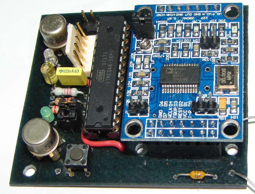
The very first design was based on AD9850 DDS chip and AtTiny26 controller. It works surprisingly well, but there are some points that can be improved. So I prepared the 2nd version, based on AD9851 and AtMega8 chip. The changes are: AD9851 can operate with DDS clock up to 180 MHz that allows to generate 50 MHz signal much cleaner than AD9850 (max. clock 125 MHz). AtMega8 contains an USART that directly implements serial port and allows to connect GPS receiver, larger EEPROM for other data... It also allows possible further features (spare IO pins, analog/digital converter for measurements etc.)
First version, CW only beacon
Its operation is quite simple: when the power is on, the beacon sends a selected CW message cyclicaly on one preprogrammed frequency. In principle it uses FSK keying (transmits one freq when key is down and another one when key up).
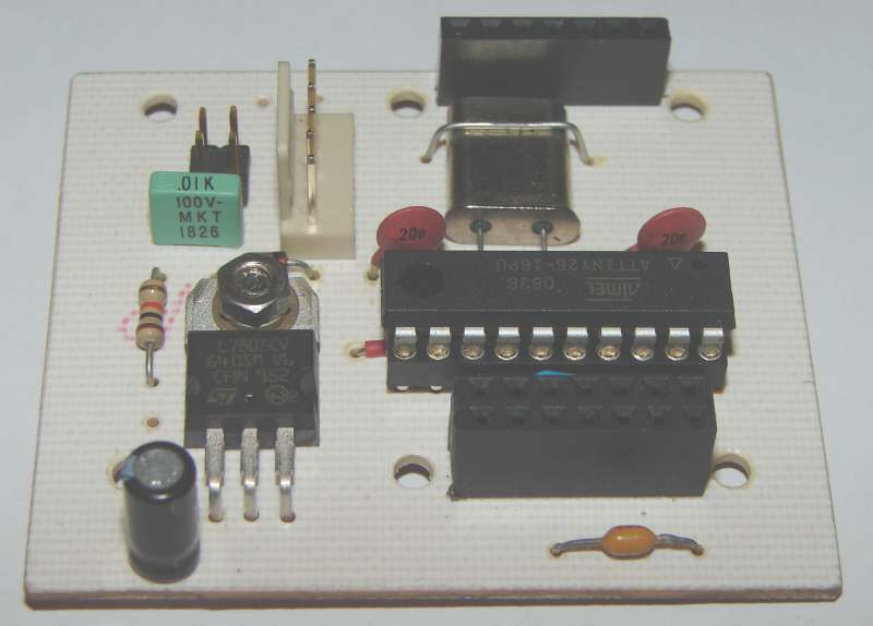
The design uses Atmel AtTiny26 controller to control 50 MHz propagation beacon - DDS control and morse keying generation (possible both CW or FSK). AVR code is written in assembler, using AVR Studio version 4. Really simple design, can be used by beginners to study the AVR assembler programming.
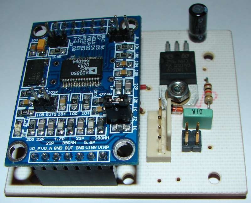
I have been inspired by a module purchased on ebay, containing Analog Device chip AD9850 (DDS generator) and all other components including 125 MHz clock crystal oscilator for reasonable price around 15 EUR from China (including postage). I don't like to work with SMD devices (too small for my eyes) so it is a nice compromise - the DDS circuitry is already done, the only thing I have to finish is the controller that I can do in classic way.
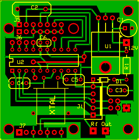
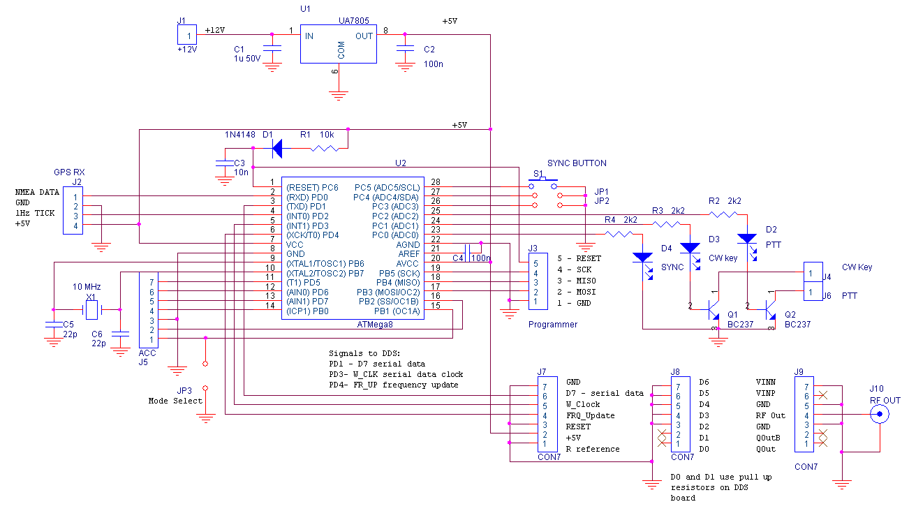
Circuit diagram
for both controller and DDS module
DDS module
It is a very simple, based on manufacturer's recommendation: DDS chip, 125 MHz XO, low path filter on the output - that's all. It is connected to "mother board" using 3 lines of pins, each line 7 pins (see the picture).
Controller
Ii is based on Atmel AVR AtTiny26, clocked by 5 MHz external crystal (frequency is not critical, it infulences just CW speed). The processor peforms just 2 main tasks: generating of morse signal (text stored in EEPROM) and downloading frequency data to DDS chip. The communication between CPU and DDS works in serial mode (the timing is not critical and serial mode reduces number of connecting wires). The CPU sends new data to DDS every time the key status (up, down) changes. It is possible to program virtualy any frequency for each of the two states, in range of 0 Hz to approx 50 MHz (must be lest than XO clock divided by two with some antialias reserve) with step of 0.03 Hz (yes, such small!). So it can be used not only on 50 MHz band but in complete HF spectrum. If you want just A1 keying and not FSK, simply program both frequencies to identical value and use pin5 port A to make keying in any following aplification stage.
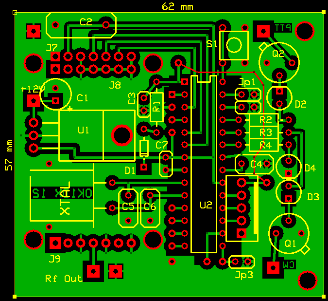
PBC prepared in ExpressPCB, version 7.0.1
Morse code generation
The beacon transmits the morse code message stored in EEPROM. The CW keying timing uses the T0 timer (cyclic interrupt). The dot length is multiple of this period, the speed constant in placed in EEPROM. The keying is possible by both methodes: A1 and F1. The text is stored in EEPROM in form 1 byte = one character, coded 0 = dot, 1 = dash, leading 1. The FSK keying is performed inside the module, A1 keying signal is available on one pin of the AVR processor.
The morse message is one of 4 fixed texts (usually beacon ID, location etc.) but some telemetry can be easily added in later versions (?).
The EEPROM capacity for texts is around 100 bytes (total length of all texts together, of course it can be just one long text or up to 4 short ones).
All version 1 sources and documentation.
Second version, HF + 50 MHz, CW + WSPR
The beacon can operate in CW or WSPR mode. It uses an internal table with 10 entries, each entry defines mode (CW or WSPR) and operating frequency. The table is processed cyclically, the switching occures every 2 minutes - the table cycle is completed in 20 minutes. The CW text can be chosen from 4 preprogrammed texts (like version 1, using jumpers), the WSPR message is one, fixed. The WSPR message is generated by program WSPRcode (K1JT), it is converted to byte format using simple utility tool.
The design supports both AD9850 and AD9851 chips (there are just 2 differencies between them - AD9851 can work faster and can use clock freq multiplier) - the selection is done when the software is compiled. AtMega8 16 MHz version chip contain USART that reads data from GPS receiver - used to adjust internal timing and sunchronisation of freq table (it uses $GPGGA sentense, 4800 Bd NMEA). When the GSP RX is not available, there is a button that allows manual synchronization at start of even minute (but this is not recommended if you want to operate the beacon over long time period). Each freq table entry contains also 3 bits that can control folowing circuitry (band or antenna switching).
The AD9851 module has been pruchased from eBay (China), the advantage is it is internally very similar to AD9850 version (just clock oscillator 30 MHz), completely pin compatible.
Result:
I was interested about the frequency stability - the requirement for 50 MHz WSPR beacon is quite high: drift less than 1 Hz during one transmission (for good performance), the long term stability must keep the beacon inside 200 Hz WSPR window. But first results are promissing - anyway, it is recommended to keep the DDS module inside closed thermo insulated box, far from sources of heat (better to move the 7805 stabilizer from PCB to heat sink, the same for power amplifier). If you supply the GPS receiver from the same stabilizer it is a must.
All version 2 sources and documentation.
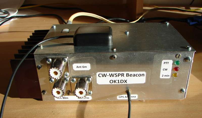
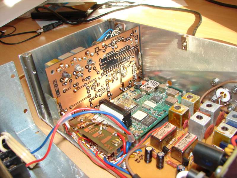
Third version, HF + 50 MHz, CW + WSPR, realization
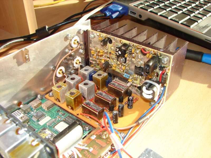
I have purchased a kit of linear 5W amplifier from Funkamateur shop (design by Harald DL2EWN). Simple design, no complicated adjustment necessary. Just the AD9851 output level is not sufficient to get a full power; additional one stage amplifier can do the job. So I have added an amplifier to the DDS mainboard. Because I plan to operate the beacon in 3 HAM bands (80, 17 and 6m), I have implemented also some kind of filter to reduce harmonics etc. There is no switching between the filters (in fact the amplifier has just slightly higher gain at that particular bands, adjustable individually for each band by a resistor), I hope is is sufficient.
The output lowpass 2 stage filters use relay switching. I found some small 5V bistabile relays in my shack that are convenient - I don't want to burn an electric power just to keep relay energized forever... So the switching circuitry is little bit more complicated than usual (each relay has 2 coils, one for each position).
The GPS receiver board is from Ebay (tks AF4JF), output set to 4800 Bd NMEA standard TTL level. It is used just to synchronize internal WSPR clock - 2 minute cycle. Battery backup is not used, as well as 1 Hz output (perhaps alter). There is a separate 7805 stabilizer for GPS receiver supply (about 150 mA)
Power supply is cheap surplus switched chinese model (rated 12V 2A).
Here you can see the beacon:
Here are some related files. I don't expect someone to build an own copy, but can be interesting...
Frequency stability
As soon as I finalized the contruction (all electronic parts, switched power supply, enclosure) I realized the circuitry inside generates significant heat that warms up the whole box. And the temperature changes have negative influence on frequency stability of DDS generator. What is quite sufficient for CW FSK and low HF bands is not enough for 50 MHz WSPR. Of course, the goal is not to drift more than 1 Hz during 2 minutes transmission and to stay in 200 Hz wide band in all situations, but it looks like the requirement is not realistic with standart XO built in the DDS module. So I searched for something better... Finally I used 16.384 MHz TCXO from old GSM BTS (thanks OK1MHK) multiplied by XOR gate to 32.768 MHz. It is slightly more than maximum 30 MHz guaranteed for AD9851, but it seems to be working fine. The TCXO can be tuned +/- 200 Hz by voltage/external potentiometer. I considered also possible PLL to GPS 1 Hz signal (the PCB is ready for that), but I found the basic stability of TCXO is sufficient. Maybe later... So the output of 30 MHz XO at the module is disconnected (a 100 ohm resistor in series at the ouput is removed) and 32 MHz is connected instead. As the next step I removed the switched power supply from the box that generated significant amount of heat, that helps the stability es well, and I operate it from external PS.
73 OK1DX